|
The uMODBUS software is designed to operate within the GPC(b) hardware, once installed if the unit is connected to a MODBUS master via the serial port. It will respond to read/write operations to the locations indicated below. Read or Write operations to locations not within this range will receive read or write exceptions from the device.
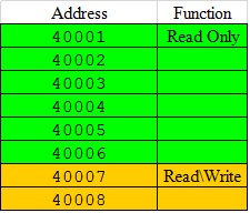
The function of each register to some extent is configurable though the jumper links on the GPC(b) board, but broadly speaking the registers have the predefined functions as below:

Before we go into detail regarding how each register can be used, let us first outline the way in which the links mentioned above alter the operation of the uMODBUS software. The functions of each of the links can be summarised as:
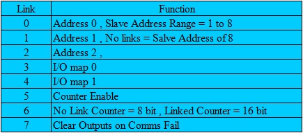
Here -
Links 0-2:
Are used to alter the slave address of the device and allow an address range of 1 to 8.
Here if no links are made an address of 8 is assumed for the device as 0 is not a
valid slave address within the MODBUS communications protocol.
Links 3/4:
Set the digital input and output mapping from the physical I/O of the GPC(b) board to
the internal MODBUS registers, the specific mapping will be discussed shortly.
Links 5/6:
Enable the frequency/pule counting feature of the uMODBUS(s) software and allow 8
or 16 bit operation to be selected.
Link 7:
If this link is made then on communications failure to the master device the outputs of the GPC(b) are automatically cleared down.
It is probably important to note that the configuration of these links is only read once at startup and so in order for any alteration in their settings to take effect the power to the core must be sequenced.
DIO (40001 & 40007):
As the board only has 16 physical digital I/O lines, tagged DIO15-DIO0 their functions must be shared between the digital input word 40001 and the digital output word 40007.
Each of the maps as configured by jumpers 3/4 are shown below, as can be seen here this sharing is done in 4 bit groups (nibbles). This results in the logical states from configured digital inputs being deposited into the 40001 MODBUS address and mapped bits from the 40007 address being passed though to physical outputs.
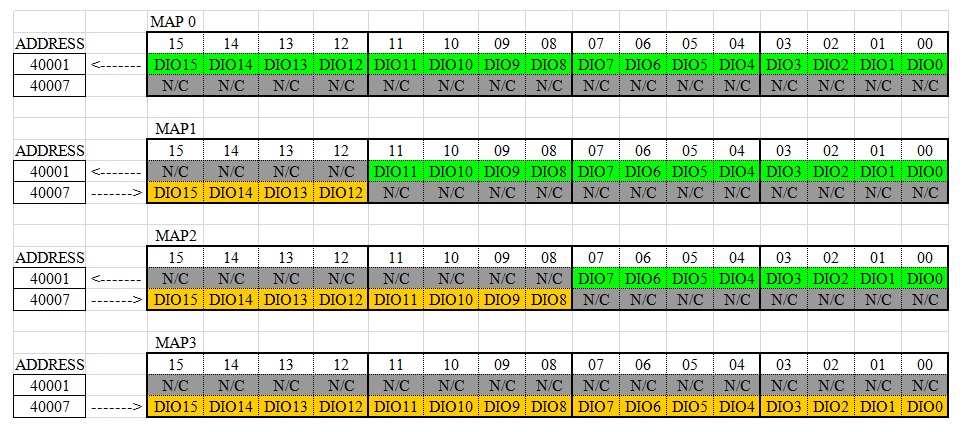
On I/O map 1, the first 12 physical inputs DIO0-DIO11 and are mapped to bits 0 to 11 of 40001 and so logical input changes to these pins will be reflected in the contents of the 40001 register. The rest of the bits in this word are unassigned and effectively have no function.
At the same time the last 4 bits of 40007 (bits 12 to 15) are mapped though to the DIO12-DIO15 physical outputs, making logical changes to these last four bits of the 40007 register will be directly reflected on the physical outputs of the board. Once again the rest of the bits in the 40007 word will not be assigned physical outputs so setting them will have no effect.
Ai0 to Ai2 (40002,40003,40004):
The function of registers 40002,40003 and 40004 are tied to analogue inputs AI0,AI1 and AI2 respectively. Each of which employs the internal 12 bit successive approximation ADC which has been configured to accept an active input range of 0-5V.
In practical terms this means an input voltage change of 0 to 5 volts on the AI0 pin will result in the contents of the 40002 register changing from 0 to 4096.
Following on from this the voltage applied to AI1 will effect the 40003 register and AI2 40004.
Pulse/Frequency Counter (40006):
If the input counter operation is selected via links 6/7, the contents of 40006 will change as the
frequency of the pulses applied to the pulse gate interface board varies with time.
The active range of the counter can be set to 8 or 16 bit operation resulting in a maximum counter range of 255 or 65535.
Extended Function Registers (40006/40008):
In version 1.01 of the uMODBUS software only the MSB of the input register 40006 is configured to contain a watchdog signal, this alternates on each successive read operation from the master device and can be used by the master as a means of ensuring the slave is present and running.
All the other bits of the 40006 register are currently unused and free for future development as too are all the bits of the 40008 output register.
LCD outputs and keyboard links:
If the LCD is fitted to the GPC(b) then it can be used to confirm basic configuration information as well as to display live system data.
On startup the boot screen indicates the build of software that is running within the microcontroller.
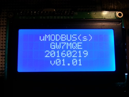
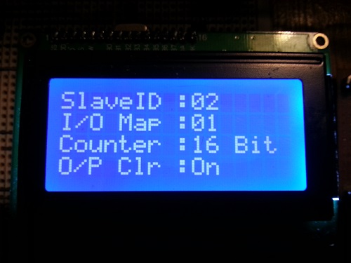
Next after a short time the configuration of the links can be verified.
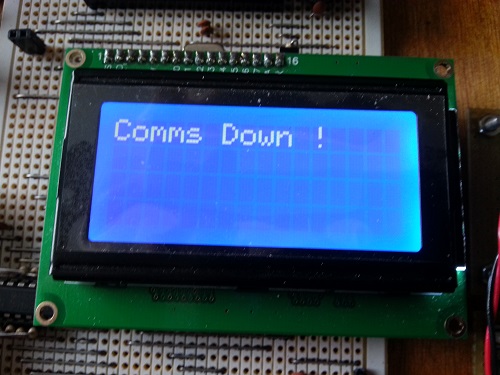
Following this if communications is not established by the master then a final default message will be shown.
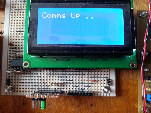
However once communications are established by the master device, by default the LCD will go blank. If further information is required then additional inputs must be made to the GPC(b) board.
To enable this function the link board (currently used on the prototype board and described at
the bottom of GPC I/O) must be fitted and at least one of the links must be made.
The link functions are summarised here:
link 1 - unused
link 2 - show RX buffer
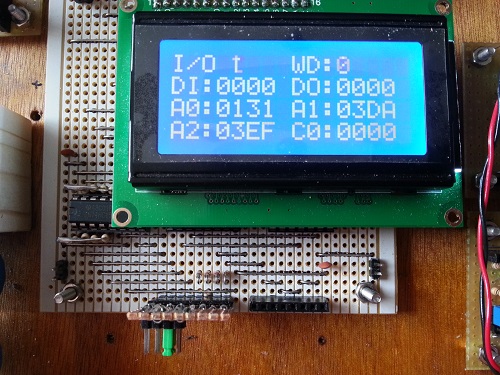
link 3 - show live I/O data
link 4 - show basic comms info
making these links results in the following LCD screens being generated.
Link 4 made - Basic Comms Info Screen
Link 3 made - Live Data Screen
Link 2 made - RX Buffer Screen

The uMODBUS(s) software operating within the GPC(b) creates a general purpose MODBUS slave platform that will aid in the development of my next project.
This will be a general purpose portable pocket SCADA solution called uSCADA(p).
Click here for the files associated with this software
|